Overview
Temperature characteristic evaluation from -60 °C to +350 °C
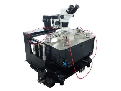
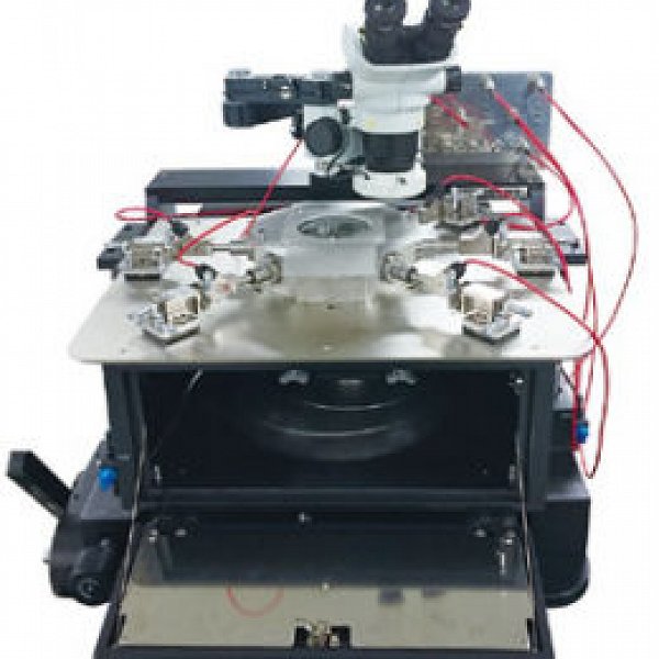
- It is a Manual Probe System which supports wafer sizes of 8 inch and 12 inch respectively.
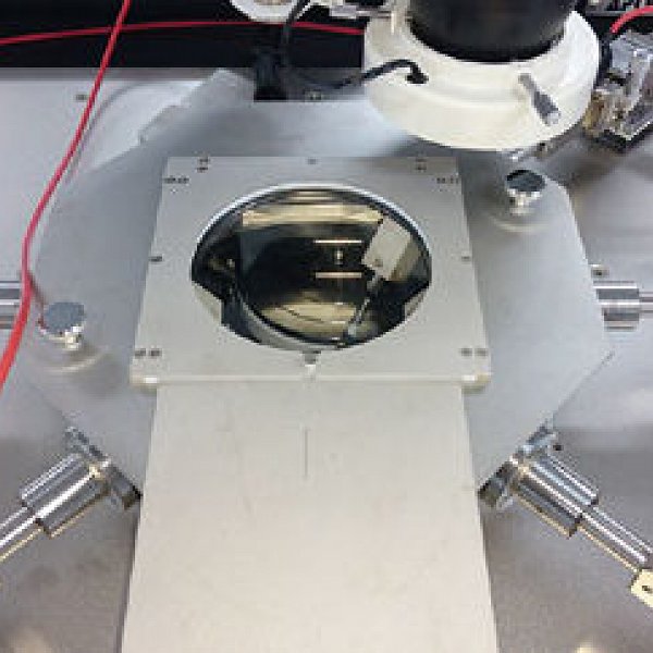
- It has a compact shield to prevent dew condensation.
- The compact shield provides a low noise environment.
- With XY coarse movement and fine adjustment using micrometer that can be quickly positioned by air bearing design, reliable alignment is possible.
- Z movement of the platen has coarse movement that can be operated with a lever, and fine movement that can be adjusted with micrometer.
Applications
- Low level IV (fA)
- Low level CV (fF)
- Probe solution for high-power devices 20kV DC/200A
- RF measurement
- Various resistance measurements such as sheet resistance
- Temperature characteristic test in high and low temperature environment
- Reliability test such as TDDB
Options
- Thermal chuck from -60°C to +350°C
- Triaxial connection to chuck
- High-power chuck
- Change to use CCD camera
- Probe card (4 .5 inch square PCB)
- Combination with various light sources
Optical System Selection
- Stereomicroscope (default)
- Trinocular microscope
- Zoom micro CCD camera
- Mitutoyo Finescope FS70Z series and FZ70L
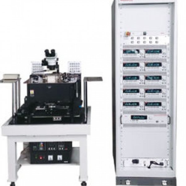
Examples of measuring instruments to be connected
- Device Analyzers/Parameter analyzers
- Power Device Analyzer
- Source Measure Units
- Curve Tracers
- Precision LCR meters
- Digital multimeters
- Impedance Analyzers
- Network Analyzers
- In addition, various measuring instruments of each company
Specifications
| α200CS | α300CS | |
|---|---|---|
| Wafer chuck size | ~8inch | ~12inch |
| Stage travel range (Coarse) | X:200㎜ Y:200㎜ | X:320㎜ Y:320㎜ |
| Stage travel range (Fine) | X:±12.5㎜ Y:±12.5㎜ | X:±12.5㎜ Y:±12.5㎜ |
| Stage θ travel | ±5° | ±4° |
| Z Stage travel | 0ー0.3ー5㎜ | 0ー0.3ー5㎜ |
| Z Stage fine travel | 10㎜ | 10㎜ |
| Dimensions | W690×D780×H620㎜ | W965×D930×H700㎜ |
| Weight | 80㎏ | 165㎏ |
Gallery


